 |
Surface/Interface Engineering of Semiconductors for Device Application"Often, it may be said that the interface is the device" ----Herbert Kroemer (2000 Nobel Prize for Physics) |
 | |||||||
| Updated: Wednesday, 29.06.2011 | Home | Members | Research | Facilities | Publications | Conference | Activity | Contact | 中文版 |
| HOME |
|---|
| MEMBERS |
| RESEARCH |
| FACILITIES |
| PUBLICATIONS |
| CONFERENCE |
| ACTIVITY |
| CONTACT US |
 |
| Thin film growth and preparation equipment | |
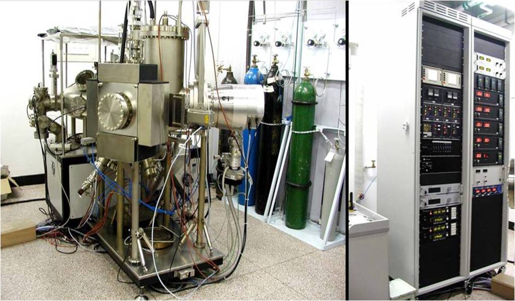
| 1. Ultra-high Vacuum Radio Frequency Plasma Assisted Molecular Beam Epitaxy System (UHV-RF-MBE) | |
 |
1. RHEED in-situ 2. 3. |
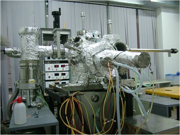
| 2. Ultra-high vacuum in situ MBE-STM system (UHV-MBE-STM) | |
 |
1. 2. 3. |
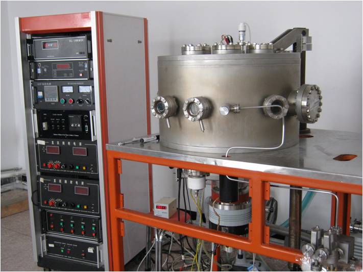
| 3. Magnetron Sputtering System (MSS) | |
 |
1. 2. 3. |
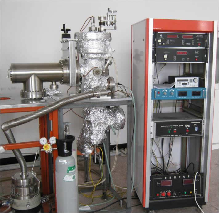
| 4. Thermal Evaporation System (TES) | |
 |
1. 2. 3. |
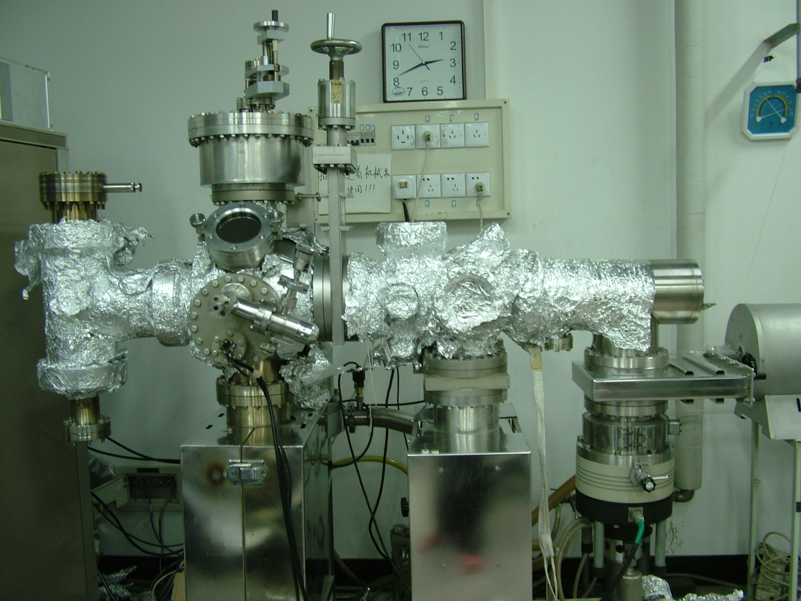
| 5. Ultra-high Vacuum System (UHV) | |
 |
1. 2. 3. |
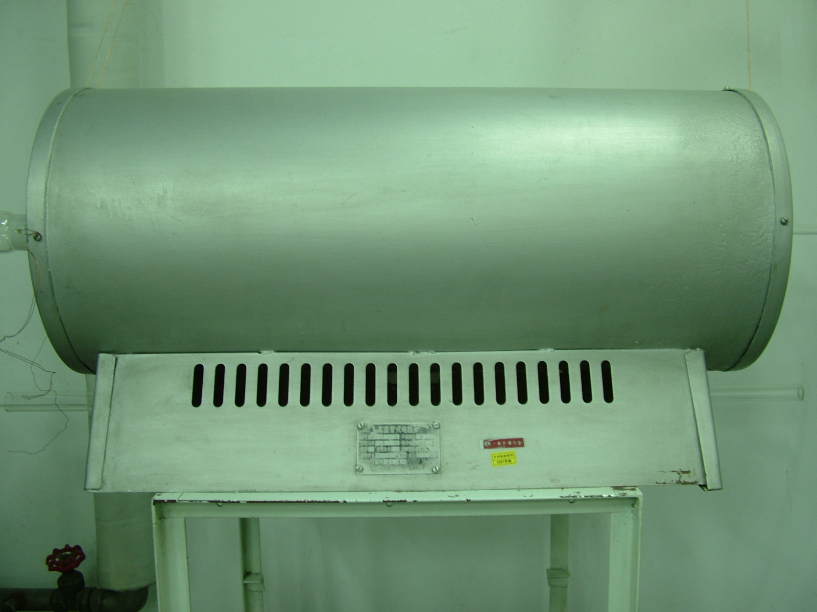
| 6. High-temperature furnace tube | |
 |
1. 2. 3. |
| Thin films and device testing equipment | |
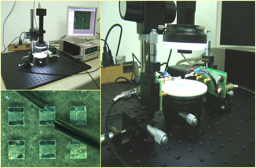
| 1. Ultra-Violet Response Test System (UV-RTS) | |
 |
1. 2. 3. |
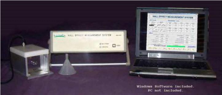
| 2. Hall test instruments (Ecopia HMS-3000) | |
 |
1. 2. 3. |
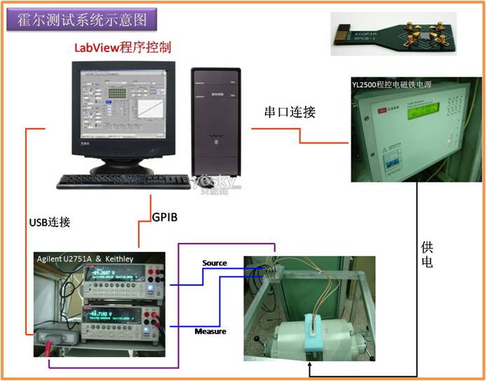
| 3. A homemade automatic four-probe Hall measurement system (EMO-600,IPCAS) | |
 |
1. 2. 3. |
|
 |